PCB Design Practice Test
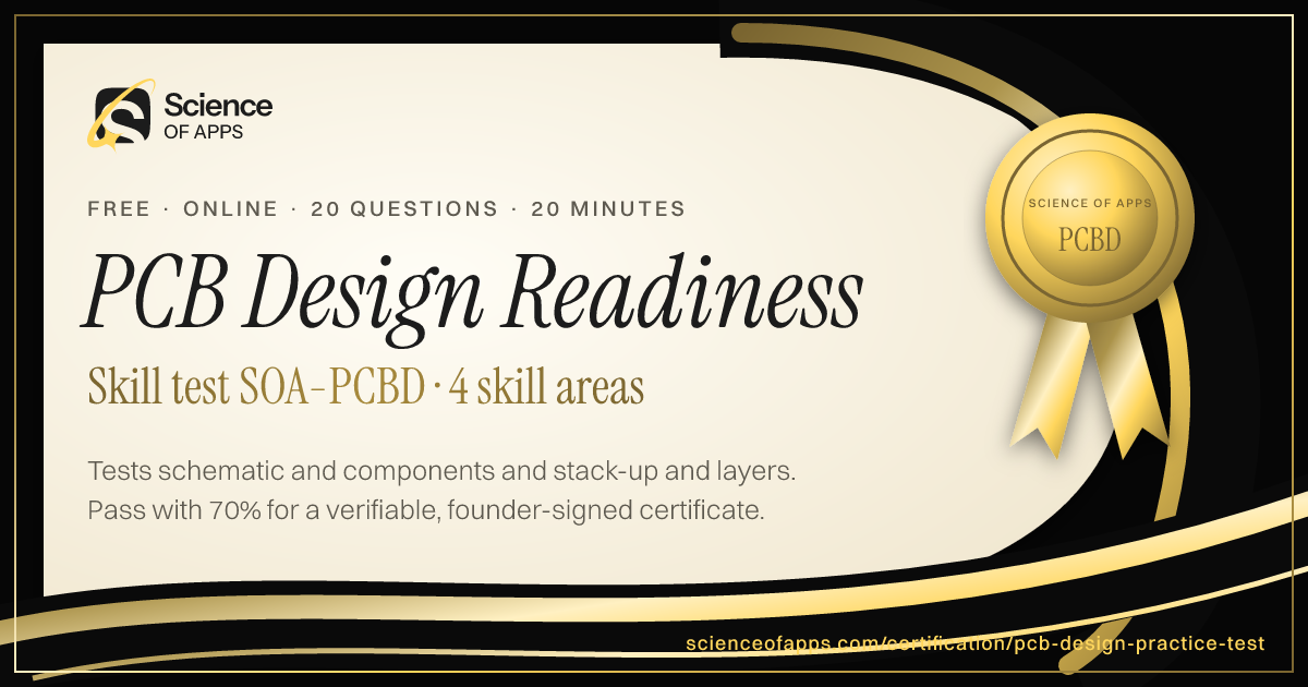
Practice for printed circuit board (PCB) design — schematic capture and nets, the PCB stack-up, layers and materials, component placement, routing, trace width and impedance, design for manufacturability, signal and power integrity and EMC, and Gerber output and assembly files — written to IPC standards including IPC-2221 and IPC-A-610, Altium and KiCad documentation for 2026. Pass to earn PCB Design Readiness SOA-PCBD.
- Intermediate difficulty.Assumes hands-on experience in the role.
- 20 scenario questions
- 20 minutes, timed
- 70% to pass · 90% for distinction
- Free no sign-up needed
- LinkedIn-ready · add it to your profile in one clickSee how ↓

 Founder, Science of Apps
What is the PCB Design Practice Test?
- Quality Assured
- Exclusive Certification
Updated for 2026 and 2027 exams. Covers schematic and components, stack-up and layers, placement and routing and manufacturing, integrity and output.
The PCB Design Practice Test is a free intermediate-level, 20-minute skill test from Science of Apps. Practice for printed circuit board (PCB) design — schematic capture and nets, the PCB stack-up, layers and materials, component placement, routing, trace width and impedance, design for manufacturability, signal and power integrity and EMC, and Gerber output and assembly files — written to IPC standards including IPC-2221 and IPC-A-610, Altium and KiCad documentation for 2026. Score 70% or more on its 20 questions to earn a verifiable PCB Design Readiness certificate (SOA-PCBD). Every question is based on published standards and research — including IPC-2221 Generic Standard on Printed Board Design (Global Electronics Association (IPC)), Altium Designer documentation (Altium), KiCad EDA documentation (KiCad) — and each answer is explained with its source.
Built for your job title
PCB designer or layout engineer, Hardware or electronics engineer, Electrical design technician, EDA tool user and Electronics student — and anyone who wants quick, verifiable proof of PCB Design knowledge for a CV or LinkedIn in 2026 and 2027.
- PCB designer or layout engineer
- Hardware or electronics engineer
- Electrical design technician
- EDA tool user
- Electronics student
What the test covers
Four skill areas with 5 questions each, drawn from a bank of 10 per area, so a retake brings questions you haven't seen.
Schematic and Components
25%- Schematic
- Nets
- Footprints
Stack-up and Layers
25%- Layers
- Materials
- Planes
Placement and Routing
25%- Placement
- Trace width
- Vias
Manufacturing, Integrity and Output
25%- DFM
- SI/PI/EMC
- Gerbers
It is a knowledge and exam-readiness test: it does not replace official certification, licensure, supervised clinical or practical training, or local regulations.
Based on published standards
The questions are original scenarios, and each one names the public standard, official guide or research it draws on — shown under the question while you answer, and linked in your review. These are the sources behind this test:
Try a sample question
The design document that defines how components connect electrically is the
- Gerber file
- schematic
- bill of materials
- stack-up only
Show the answer
B. schematic — Schematic. The real test has 20 questions like this.
How the test works
20 minutes, 20 questions
One question per screen, with a progress bar and a countdown. Your progress is saved on this device if you need to pause.
Graded on our server
Answers reach the page only after you submit, so the certificate can only be earned by passing.
Every answer explained
Pass or not, you see every question with the right answer, why, and the source behind it. Pass mark 70%, distinction 90%.
Your certificate
Founder-signed, with a QR code and credential ID. Download PDF or PNG, add to LinkedIn, and it's emailed to you.
What you earn
Pass, then add it to LinkedIn in one click
No typing. The Add to LinkedIn button opens your profile’s Licenses & certifications form already filled in: the certificate name, Science of Apps as the issuer, the issue date, your credential ID and a link recruiters can use to verify it.
- 1Take the 20-minute test
- 2Score 70% or more
- 3Click Add to LinkedIn

PCB Design Readiness
Science of Apps
Show credential ↗Try another skill test
- 20 minSOA-MECH
Mechanical Engineering Practice Test (FE-Style)
Tests mechanical engineering fundamentals in the style of the FE Mechanical exam — statics and mechanics of materials, thermodynamics and heat transfer, fluid mechanics, and dynamics, machine design and materials — with worked calculations.
Difficulty: AdvancedTake the 20-minute test → - 20 minSOA-ELEC
Electrical Engineering Practice Test (FE-Style)
Tests electrical and computer engineering fundamentals in the style of the FE Electrical and Computer exam — circuit analysis, electronics and digital logic, power systems and machines, and signals, control and communications.
Difficulty: AdvancedTake the 20-minute test → - 20 minSOA-CIVL
Civil Engineering Practice Test (FE-Style)
Tests civil engineering fundamentals in the style of the FE Civil exam — structural analysis and materials, geotechnical engineering, water resources and environmental engineering, and transportation and construction — with worked calculations.
Difficulty: AdvancedTake the 20-minute test →
Frequently asked questions
What is the PCB Design Practice Test?
The PCB Design Practice Test is a free intermediate-level, 20-minute skill test from Science of Apps. Practice for printed circuit board (PCB) design — schematic capture and nets, the PCB stack-up, layers and materials, component placement, routing, trace width and impedance, design for manufacturability, signal and power integrity and EMC, and Gerber output and assembly files — written to IPC standards including IPC-2221 and IPC-A-610, Altium and KiCad documentation for 2026. Score 70% or more on its 20 questions to earn a verifiable PCB Design Readiness certificate (SOA-PCBD). Every question is based on published standards and research — including IPC-2221 Generic Standard on Printed Board Design (Global Electronics Association (IPC)), Altium Designer documentation (Altium), KiCad EDA documentation (KiCad) — and each answer is explained with its source.
Is there a free PCB Design practice test for 2026?
Yes. Science of Apps has a free PCB Design Practice Test built on the current exam outline for 2026 and 2027. It covers schematic and components, stack-up and layers, placement and routing and manufacturing, integrity and output, scores you instantly and issues a verifiable certificate.
How do I take the PCB Design Practice Test for free?
Read the four skill areas on this page, then take the 20-minute test online — no fee, course or sign-up. You see every answer explained when you finish. Score 70% or more and you get a PCB Design Readiness certificate straight away, on screen, as a PDF and by email, with a credential ID anyone can verify.
Are the PCB Design Practice Test questions based on real standards?
Yes. The questions are original scenarios written by Science of Apps, and each one is based on a public source you can read: IPC-2221 Generic Standard on Printed Board Design (Global Electronics Association (IPC)); Altium Designer documentation (Altium); KiCad EDA documentation (KiCad); Acceptability of Electronic Assemblies (IPC-A-610J-2024) overview (ANSI). The source is shown under each question and linked in the answer review. Science of Apps doesn't copy questions from other tests.
What does the PCB Design Practice Test cover?
Four skill areas with five questions each, drawn from a bank of 10 per area so a retake brings new questions: Schematic and Components (Schematic, Nets and Footprints); Stack-up and Layers (Layers, Materials and Planes); Placement and Routing (Placement, Trace width and Vias); Manufacturing, Integrity and Output (DFM, SI/PI/EMC and Gerbers). Every question is an original scenario written to the 2026–2027 standard, with the published source named under it.
Who should take the PCB Design Practice Test?
PCB designer or layout engineer, Hardware or electronics engineer, Electrical design technician, EDA tool user and Electronics student. It suits anyone who wants a quick, verifiable way to show PCB Design knowledge in 2026 and 2027, from students and career switchers to experienced professionals.
What standards govern PCB design?
IPC publishes the key standards: IPC-2221 for generic PCB design, IPC-2222 for rigid boards, IPC-A-610 for acceptability of assemblies and J-STD-001 for soldering. Designers also follow their fabricator's capabilities and tool documentation.
What is a PCB stack-up?
A stack-up is the arrangement of copper and insulating (dielectric) layers through the thickness of the board. It sets the number of signal, power and ground layers, their order and spacing, which affects impedance, signal integrity and manufacturability.
Can I take the PCB Design Practice Test from any country?
Yes. The test is online, in English and free everywhere — people take it from India, the US, the UK, Europe, Africa, Latin America and Asia-Pacific. Your certificate is dated with your own local date and can be verified from anywhere at scienceofapps.com/certification/verify/.
How long is the PCB Design Practice Test?
20 questions — 5 from each of 4 skill areas — with a 20-minute limit. You need 70% (14 of 20) to pass and 90% for distinction.
How hard is the PCB Design Practice Test?
We rate it Intermediate: assumes hands-on experience in the role. It has 20 scenario questions — 5 from each of 4 skill areas — and a 20-minute limit. You need 70% (14 of 20) to pass and 90% for distinction.
How much do Science of Apps certifications cost?
Nothing. There is no fee to take a test, to receive the certificate, to have it emailed or to verify it, and no sign-up.
How are the tests graded?
On our server, not in your browser. The answers never reach the page until you submit, so a certificate can only be earned by passing. Each certificate gets a unique credential ID stored by Science of Apps.
What happens if I don't pass?
You see your score for each area and every question with the correct answer and why, with the published source behind it. You can retake after 30 minutes, and the retake draws questions you haven't seen yet.
Do the certificates expire?
No. Every certificate is dated, so it always shows when you passed. Retake a test any time for a newer date or a higher score.
Can I add the certificate to LinkedIn?
Yes. After you pass, Add to LinkedIn opens the Licenses & certifications form with the certificate name, Science of Apps as the issuer, the issue date, your credential ID and the verification link filled in. You can also download it as a PDF or PNG, and it's emailed to you as a PDF.
How can an employer verify my certificate?
Every certificate has a credential ID and a QR code. Scanning it, or entering the ID at scienceofapps.com/certification/verify/, shows the holder's name, the certification, the score and the issue date from our records.
Are these accredited qualifications?
No. They are Science of Apps' own assessments of applied skill. They aren't issued by a university or standards body, and they work best alongside a portfolio that shows the skills in real work.
2402 more certifications to collect
Engineering, Architecture, Construction & Safety
- Mechanical Engineering Practice Test (FE-Style)20 min · Advanced
- Electrical Engineering Practice Test (FE-Style)20 min · Advanced
- Civil Engineering Practice Test (FE-Style)20 min · Advanced
- Chemical Engineering Practice Test (FE-Style)20 min · Advanced
- Engineering Mathematics Practice Test15 min · Intermediate
- CAD Certification10 min · Beginner
- AutoCAD Certification Practice Test15 min · Intermediate
- SolidWorks Certification Practice (CSWA-Style)15 min · Intermediate
- Revit Certification Test (Revit & BIM)15 min · Intermediate
- HVAC Certification Practice Test15 min · Intermediate
- PLC Programming Certification15 min · Intermediate
- Industrial Maintenance Certification15 min · Intermediate
- Quality Control Certification15 min · Intermediate
- Lean Manufacturing Certification15 min · Intermediate
- ISO 9001 Certification Training15 min · Intermediate
- ISO 14001 Certification Training15 min · Intermediate
- Occupational Health & Safety (OHS) Certification15 min · Intermediate
- OSHA Practice Test (10-Hour & 30-Hour Topics)15 min · Intermediate
- NEBOSH Practice Questions20 min · Advanced
- Fire Safety Certification10 min · Beginner
- Electrical Safety Certification (NFPA 70E-Aligned)15 min · Intermediate
- Construction Project Controls Certification20 min · Advanced
- Quantity Surveying Certification15 min · Intermediate
- Construction Procurement & Contracts Certification15 min · Intermediate
- Fleet Safety Certification10 min · Beginner
- Revit Architecture Skills Test15 min · Intermediate
- BIM Coordinator Certification20 min · Advanced
- Building Codes Certification (IBC-Aligned)15 min · Intermediate
- Architectural Design Certification15 min · Intermediate
- Building Energy Modeling Certification20 min · Advanced
- Industrial Automation Certification20 min · Intermediate
- Construction Management Certification20 min · Intermediate
- Plumbing Test15 min · Beginner
- Welding Test15 min · Beginner
- Robotics Certification20 min · Intermediate
- Manufacturing Processes Test20 min · Intermediate
- Materials Science Test20 min · Intermediate
- LEED Green Associate Practice Test20 min · Intermediate
- CNC Machinist Test20 min · Intermediate
- GD&T Test25 min · Advanced
- Electrical Aptitude Test15 min · Beginner
- GHS Training Quiz15 min · Beginner
- Forklift Certification Test15 min · Beginner
- Electrician Practice Test (NEC 2026)20 min · Intermediate
- Fusion 360 Certification Test20 min · Intermediate
- A&P Mechanic Practice Test (General, Airframe & Powerplant)20 min · Intermediate
- PE Exam Practice Test25 min · Advanced
- IOSH Managing Safely Practice Test15 min · Beginner
- ASQ CQE Practice Test (Quality Engineer)25 min · Advanced
- ASQ CQA Practice Test (Quality Auditor)20 min · Intermediate
- CSP Practice Test (Certified Safety Professional)25 min · Advanced
- F-Gas Practice Test20 min · Intermediate
- FE Exam Practice Test20 min · Intermediate
- NICET Fire Alarm Practice Test20 min · Intermediate
- EV Charger Installation Certification Test20 min · Intermediate
- ACCA Manual J Practice Test20 min · Intermediate
- Fall Protection Certification Test15 min · Beginner
- Siemens NX Certification Test20 min · Intermediate
- Industrial Engineering Certification Test20 min · Intermediate
- Rigging Practice Test (NCCCO Rigger)20 min · Intermediate
- Statistical Process Control Certification Test (SPC)20 min · Intermediate
- EHS Certification Test20 min · Intermediate
- Health and Safety Level 2 Practice Test15 min · Beginner
- Confined Space Certification Test15 min · Beginner
- API 510 Practice Test (Pressure Vessel Inspector)25 min · Advanced
- NDT Practice Test (UT, MT, PT & VT)20 min · Intermediate
- RTL Design with Verilog & SystemVerilog Certification25 min · Advanced
- Semiconductor Fabrication & Process Engineering Certification25 min · Advanced
- Battery & Energy Storage Engineering Certification25 min · Advanced
- Chip Verification Engineer Certification25 min · Advanced
- EV Powertrain Engineering Certification25 min · Advanced
- Data Center Power & Cooling Engineering Certification20 min · Intermediate
- Green Hydrogen & Electrolyzer Technology Certification20 min · Intermediate
- Aerospace Engineering Certification Test (Fundamentals)20 min · Intermediate
- Control Systems Engineering Certification20 min · Intermediate
- Digital Signal Processing Certification20 min · Intermediate
- Medical Device Design & Human Factors Certification25 min · Advanced
- UAV Certification Test20 min · Intermediate
- Motorsport Engineering & Race Strategy Certification20 min · Intermediate
- HACCP Certification Practice Test20 min · Intermediate
- Bloodborne Pathogens Certification15 min · Beginner
- AWS Welding Certification Practice Test20 min · Intermediate
- CHST Practice Test20 min · Intermediate
- BREEAM Practice Test20 min · Intermediate
- FMP (Facility Management Professional) Practice Test20 min · Intermediate
- AMPP (NACE) Coating Inspector Practice Test20 min · Intermediate
- ASE Certification Practice Test20 min · Intermediate
- BOSIET Practice Test (Offshore Safety Induction)20 min · Intermediate
- FSSC 22000 Practice Test (Version 6)20 min · Intermediate
- HAZWOPER Practice Test15 min · Beginner
- IPC-A-610 Practice Test20 min · Intermediate
- GWO Basic Safety Training Practice Test20 min · Intermediate
- Passive House Certification20 min · Intermediate
- Solar PV (NABCEP) Practice Test20 min · Intermediate
- Scaffolding Certification20 min · Intermediate
- ANSYS Practice Test25 min · Advanced
- Carpentry Certification15 min · Beginner
- Land Surveying Certification20 min · Intermediate
- Anti-Bribery ISO 37001 Practice Test20 min · Intermediate
- Diesel Mechanic Certification20 min · Intermediate
- CATIA Practice Test20 min · Intermediate
- HERS Energy Rater Practice Test20 min · Intermediate
- Horticulture Certification20 min · Intermediate
- ISO 26262 Practice Test25 min · Advanced
- OHST Practice Test20 min · Intermediate
- Wastewater Certification20 min · Intermediate
- Cathodic Protection Certification20 min · Intermediate
- NATE HVAC Practice Test20 min · Intermediate
- Building Operator Certification20 min · Intermediate
- IEC 61508 Functional Safety Practice Test25 min · Advanced
- Marine Engineering Certification20 min · Intermediate
- Millwright Certification20 min · Intermediate
- Painting and Decorating Certification20 min · Intermediate
- Process Safety Management Certification20 min · Intermediate
- Root Cause Analysis for Operational Failures Certification20 min · Intermediate
- Stick Welding Certification20 min · Intermediate
- TIG Welding Practice Test20 min · Intermediate
- IATA Dangerous Goods Regulations (DGR) Practice Test20 min · Intermediate
- FANUC Robot Operation and Programming Practice Test20 min · Intermediate
- Total Quality Management (TQM) Practice Test20 min · Intermediate
- Blueprint Reading Certification20 min · Intermediate
- Masonry Certification20 min · Intermediate
- Agronomy Certification20 min · Intermediate
- DCS Systems Practice Test20 min · Intermediate
- Welding Symbols Certification20 min · Intermediate
- ASQ CQT Practice Test20 min · Intermediate
- Altium Designer Certification20 min · Intermediate
- FMEA Practice Test20 min · Intermediate
- Industrial Electrician Certification20 min · Intermediate
- Manual Handling Certification20 min · Intermediate
- ASNT Level III Practice Test25 min · Advanced
- CSHM Practice Test20 min · Intermediate
- Metrology Practice Test20 min · Intermediate
- Reverse Engineering Practice Test20 min · Intermediate
- APQP Practice Test20 min · Intermediate
- COSHH Practice Test20 min · Intermediate
- Concrete Finishing (ACI) Practice Test20 min · Intermediate
- Electric Vehicle Technician Practice Test15 min · Beginner
- PPAP Practice Test20 min · Intermediate
- Value Engineering Practice Test20 min · Intermediate
- Archicad Practice Test20 min · Intermediate
- CPC Constructor Practice Test20 min · Intermediate
- Construction Scheduling Practice Test20 min · Intermediate
- Rigger and Signal Person Certification20 min · Intermediate
- Abaqus Certification20 min · Intermediate
- Asphalt Certification20 min · Intermediate
- ETABS Practice Test20 min · Intermediate
- Plumbing Design Practice Test18 min · Beginner
- STAAD.Pro Practice Test20 min · Intermediate
- Value Stream Mapping Certification20 min · Intermediate
- GMP (Good Manufacturing Practice) Practice Test20 min · Intermediate
- ISO 45001 Practice Test20 min · Intermediate
- AS9100 Practice Test20 min · Intermediate
- SQF Practitioner Practice Test20 min · Intermediate
- CMRP Practice Test25 min · Advanced
- ISO 22000 Practice Test20 min · Intermediate
- CWI (Certified Welding Inspector) Practice Test20 min · Intermediate
- IATF 16949 Practice Test20 min · Intermediate
- BRCGS Food Safety Practice Test (Issue 9)20 min · Intermediate
- Arborist Certification20 min · Intermediate
- Certified Energy Manager (CEM) Practice Test20 min · Intermediate
- Industrial Hygiene (CIH) Practice Test25 min · Advanced
- Thermography Certification20 min · Intermediate
- ISO/IEC 17025 Practice Test20 min · Intermediate
- LEED AP BD+C Practice Test20 min · Intermediate
- Scissor Lift Certification15 min · Beginner
- Rope Access IRATA Practice Test20 min · Intermediate
- Aerial Lift MEWP Practice Test15 min · Beginner
- ISO 31000 Practice Test20 min · Intermediate
- CQM Quality Management Practice Test20 min · Intermediate
- ISO 20000 Practice Test20 min · Intermediate
- ADAS Practice Test20 min · Intermediate
- Excavator Certification20 min · Intermediate
- Telehandler Certification15 min · Beginner
- AACE Cost Estimator Practice Test (CEP)20 min · Intermediate
- FIDIC Practice Test20 min · Intermediate
- IPC/WHMA-A-620 Cable and Harness Practice Test20 min · Intermediate
- Maintenance Technician Certification15 min · Beginner
- IPC J-STD-001 Soldering Practice Test20 min · Intermediate
- Working at Height Certification20 min · Intermediate
- Landscaping Certification20 min · Intermediate
- MIG Welding (GMAW) Practice Test20 min · Intermediate
- 5S Practice Test20 min · Intermediate
- Cleanroom Certification20 min · Intermediate
- Instrumentation Certification20 min · Intermediate
- Mechatronics Certification20 min · Intermediate
- Oil and Gas Certification20 min · Intermediate
- Pipefitting Certification20 min · Intermediate
- Roofing Certification20 min · Intermediate
- Structural Engineering Certification20 min · Intermediate
- WELL AP Practice Test20 min · Intermediate
- Autodesk Civil 3D Practice Test20 min · Intermediate
- Ergonomics and Workstation Risk Review Certification20 min · Intermediate
- ISO 41001 Practice Test20 min · Intermediate
- Lockout Tagout Certification20 min · Intermediate
- Revit MEP Practice Test20 min · Intermediate
- Solid Edge Certification20 min · Intermediate
- Underwater Welding Certification20 min · Intermediate
- ICC Residential Building Inspector (B1) Practice Test20 min · Intermediate
- NICET Water-Based Fire Protection Practice Test20 min · Intermediate
- Vibration Analysis Certification20 min · Intermediate
- Appliance Repair Certification20 min · Intermediate
- Creo Certification20 min · Intermediate
- IWCF Drilling Well Control Practice Test20 min · Intermediate
- HAZOP Practice Test20 min · Intermediate
- Rhino 3D Practice Test20 min · Intermediate
- Wind Turbine Technician Certification15 min · Beginner
- IPC CID Practice Test20 min · Intermediate
- Hydraulics Certification20 min · Intermediate
- Phased Array UT (PAUT) Practice Test20 min · Intermediate
- CCM Construction Manager Practice Test20 min · Intermediate
- GDP Good Distribution Practice Practice Test20 min · Intermediate
- PCB Design Practice TestYou're here
- Visual Inspection (VT) Practice Test20 min · Intermediate
- Allergen Awareness Practice Test15 min · Beginner
- Commercial HVAC Practice Test20 min · Intermediate
- Drywall Practice Test20 min · Intermediate
- KiCad Practice Test20 min · Intermediate
- Root Cause Analysis (TapRooT) Practice Test20 min · Intermediate
- Workplace Safety Practice Test20 min · Intermediate
- Building Automation (BAS) Practice Test20 min · Intermediate
- Computer System Validation (CSV) Practice Test20 min · Intermediate
- Maintenance, Reliability and Failure Analysis Certification20 min · Intermediate
- Theory of Constraints Certification20 min · Intermediate
- Aspen Plus Certification20 min · Intermediate
- Confined Space Rescue Certification20 min · Intermediate
- Pipeline Integrity Profile5 min · Beginner
- Psychological Safety and Team Learning Certification20 min · Intermediate
- Tekla Certification20 min · Intermediate
Foundation
AI & Generative AI
- AI UX Design Certification30 min · Advanced
- Prompt Engineering Certification30 min · Intermediate
- AI Product Manager Certification30 min · Advanced
Software Engineering & Web Development
- HTML & CSS Certification Test10 min · Beginner
- JavaScript Certification Test (Fundamentals)10 min · Beginner
- TypeScript Certification Test (Fundamentals)15 min · Intermediate
Data Analytics & Business Intelligence
- Product Analytics Certification30 min · Advanced
- Data Literacy Certification10 min · Beginner
- Microsoft Excel Certification Test (Fundamentals)10 min · Beginner
Digital Marketing, SEO, AEO & Growth
- Conversion Rate Optimization (CRO) Certification30 min · Advanced
- App Store Optimization (ASO) Certification30 min · Intermediate
- Growth Marketing Certification30 min · Intermediate
UX/UI, Design, Research & Creative
- UX Design Certification30 min · Intermediate
- UI Design Certification30 min · Intermediate
- Product Design Certification30 min · Intermediate
Product, Project Management & Business Analysis
- Product Manager Certification30 min · Intermediate
- Design Leadership Certification30 min · Advanced
- Agile Product Owner Certification30 min · Intermediate
Cybersecurity, IT, Cloud & DevOps
- Cybersecurity Certification Test (Fundamentals)10 min · Beginner
- Security Awareness Certification Test (Phishing Detection)10 min · Beginner
- Network Security Certification Test (Fundamentals)15 min · Intermediate
Sales, Customer Success & Support
- Sales Fundamentals Certification10 min · Beginner
- Consultative Selling Certification15 min · Intermediate
- B2B Sales Development Representative Certification10 min · Beginner
Human Resources & People Management
- Human Resources Certification Test (Fundamentals)10 min · Beginner
- Talent Acquisition Certification Test10 min · Beginner
- Technical Recruitment Certification15 min · Intermediate
Finance, Accounting, Operations & Entrepreneurship
- Financial Literacy Test (for Professionals)10 min · Beginner
- Accounting Certification Test (Fundamentals)10 min · Beginner
- Bookkeeping Certification Test (Fundamentals)10 min · Beginner
Communication, Leadership & Transferable Skills
- Critical Thinking Test10 min · Beginner
- Attention to Detail Test10 min · Beginner
- Cognitive Bias Test10 min · Beginner
Languages
- English Level Test30 min · Beginner
- American Sign Language (ASL) Foundations Test25 min · Intermediate
- App & Software Localization Test25 min · Intermediate
Healthcare, Education, Legal Operations & Sustainability
- Healthcare Administration Certification Test (Fundamentals)10 min · Beginner
- Medical Office Administration Certification10 min · Beginner
- Healthcare Data Privacy Awareness Certification10 min · Beginner
Test Prep, Academics & Aptitude
- SAT Math Practice Test20 min · Advanced
- SAT Reading and Writing Practice Test20 min · Advanced
- ACT Practice Test (English, Math, Reading & Science)20 min · Advanced
Language Exam Prep
- IELTS Academic Practice Test with Band Score20 min · Advanced
- IELTS General Training Practice Test20 min · Advanced
- TOEFL iBT Practice Test20 min · Advanced
Office & Productivity Software
- Microsoft Word Skills Certification15 min · Intermediate
- Microsoft PowerPoint Skills Certification15 min · Intermediate
- Microsoft Outlook Skills Certification10 min · Beginner
Hospitality, Travel & Retail
- Hospitality Management Certification10 min · Beginner
- Food Safety Certification10 min · Beginner
- Hotel Revenue Management Certification15 min · Intermediate
Cognitive Ability & Pre-Employment Tests
- IQ Test20 min · Intermediate
- Numerical Reasoning Test20 min · Intermediate
- Verbal Reasoning Test20 min · Intermediate
Personality & Career Assessments
- Hogan Assessment Practice Test11 min · Beginner
- Big Five Personality Test10 min · Beginner
- Enneagram Test11 min · Beginner
Health, Fitness & Wellness
- Personal Trainer Practice Test (NASM, ACE & ISSA)20 min · Intermediate
- ACSM Practice Test (CPT & EP)20 min · Intermediate
- Yoga Teacher Certification Test (RYT 200)15 min · Beginner
Beauty & Cosmetology
- Nail Technician Practice Test15 min · Beginner
- Cosmetology Practice Test15 min · Beginner
- Esthetician Practice Test15 min · Beginner
Business Software, ERP & CRM
- Sage Accounting Software Certification Test20 min · Intermediate
- Salesforce Certified Associate Practice Test15 min · Beginner
- HubSpot Content Marketing Certification Practice Test20 min · Intermediate
Consulting, Strategy & Industry Leadership
- AI for Management Consultants Certification20 min · Intermediate
- Chief of Staff Certification Test20 min · Intermediate
- Market Sizing & Estimation Certification15 min · Beginner
Law, Policy & Global Affairs
- AI for Lawyers & Legal Practice Certification20 min · Intermediate
- Geopolitical Risk Analysis Certification20 min · Intermediate
- AI for Public Policy Professionals Certification20 min · Intermediate
Frontier Science & Deep Tech
- Quantum Computing Certification Test (Fundamentals)20 min · Intermediate
- Neurotechnology & Brain-Computer Interfaces Certification20 min · Intermediate
- Nuclear Fission & Fusion Energy Fundamentals Certification20 min · Intermediate
Creative Arts, Writing & Media
- Creative Writing Certification15 min · Beginner
- Game Design Certification20 min · Intermediate
- Screenwriting Certification20 min · Intermediate
Hobbies, Culture & Lifestyle
- Chess Strategy & Tactics Test15 min · Beginner
- Philosophy Fundamentals Test15 min · Beginner
- Stoic Philosophy for Modern Leaders Test15 min · Beginner
Global Business & Country Markets
- India Stack & Digital Public Infrastructure Certification20 min · Intermediate
- Indian Startup Ecosystem & Fundraising Certification20 min · Intermediate
- Indian Capital Markets Fundamentals Certification15 min · Beginner
Read before you test
- Career guidesFigma skills employers want in 2027: auto layout, components and variants, variables, prototyping, Dev Mode and working in shared filesFigma skills employers want in 2027: auto layout, components, variants, variables, prototyping, libraries, Dev Mode handoff and tidy, shared files.
- AI & vibe coding20 copy-paste AI skills for software engineers, for ChatGPT, Claude and Gemini20 free copy-paste AI skills for software engineers — stack trace debugger and more — each with an output preview and the exact text to paste.
- Career guidesHow to get a UI designer job in 2027: visual hierarchy, layout, type, colour, components, states and the portfolio that proves craftHow to get a UI designer job in 2027: hierarchy, layout, type, colour, components, states, accessibility, a craft-focused portfolio and pay in India.
- Career guidesHow to get a design systems job in 2027: tokens, components, documentation, governance, adoption and working between design and engineeringHow to get a design systems job in 2027: tokens, components, documentation, governance, adoption metrics, design-code parity, pay and a plan.
- Law of UX · Interaction & speedSteering LawThe time it takes to move a pointer through a tunnel or path depends on the path's length and width: long, narrow paths are slow and error-prone.
- Law of UX · Memory & attentionSelective AttentionPeople focus on the small part of their environment related to their current goal and filter out the rest — including things designers want them to notice.

Get the ideas, not the noise.
Sign up with Google and we’ll send you short UX psychology tips by email — why people tap, stall and leave, and what to do about it. Unsubscribe anytime. Prefer something to keep? Get the free Laws of UX guide as a PDF.